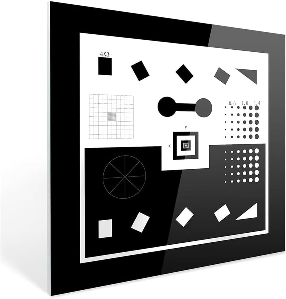
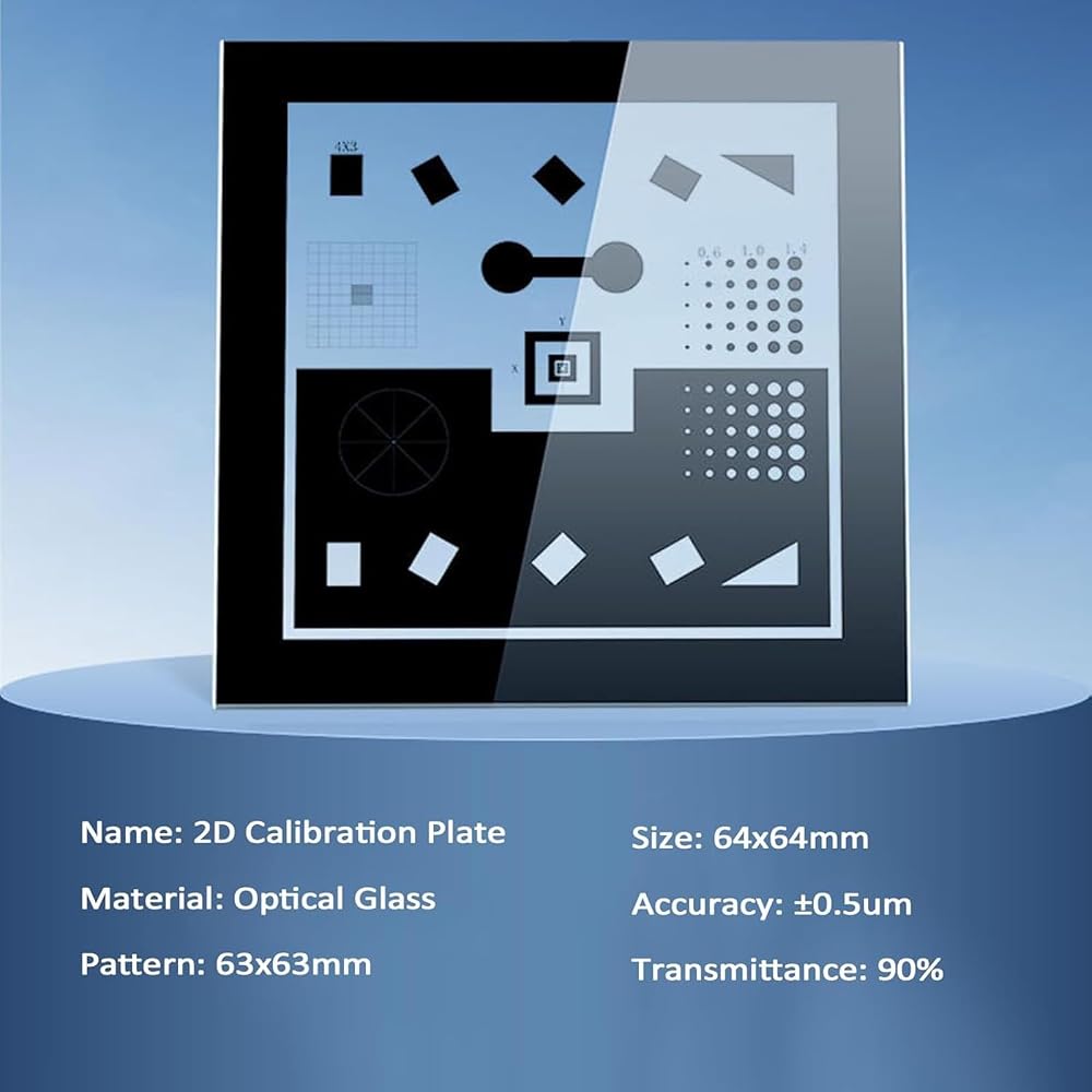
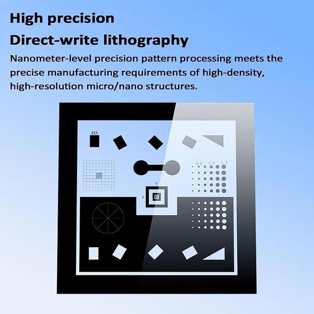
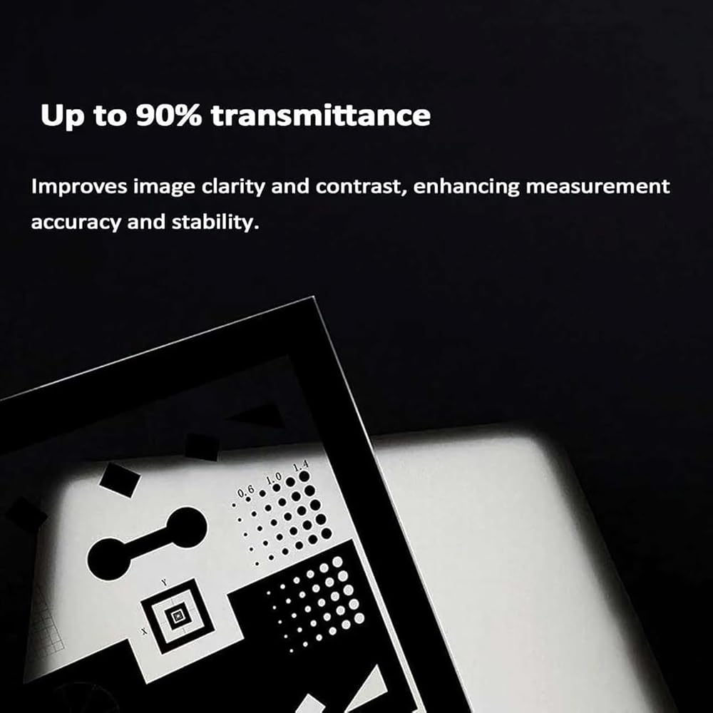
【High-Precision Nanoscale Lithography Process】: Utilizing high-precision direct-write lithography technology, it achieves precise nanoscale pattern processing, perfectly meeting the demands of high-density, high-resolution micro/nanostructure precision manufacturing and high-end calibration.
【 High optical transmittance performance】: Features outstanding light transmittance of up to 90%, effectively enhancing imaging clarity and contrast for more precise measurement results and stable system operation.
【 Stringent precision and quality control】: Capable of ±5 micron high-precision calibration combined with rigorous manufacturing process control, ensuring each calibration plate meets standard specifications for stable and reliable application in scientific research experiments and industrial inspection scenarios.
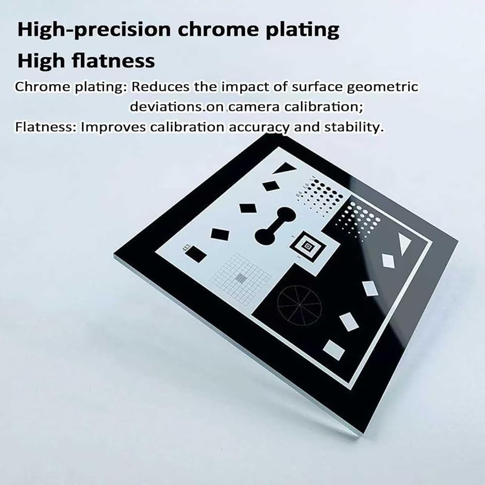
【Highly Flat Chrome-Plated Surface】: Achieves ultra-flat surfaces through uniform chrome plating, minimizing geometric surface deviations that interfere with camera calibration. This exceptional flatness further enhances calibration accuracy and long-term stability.
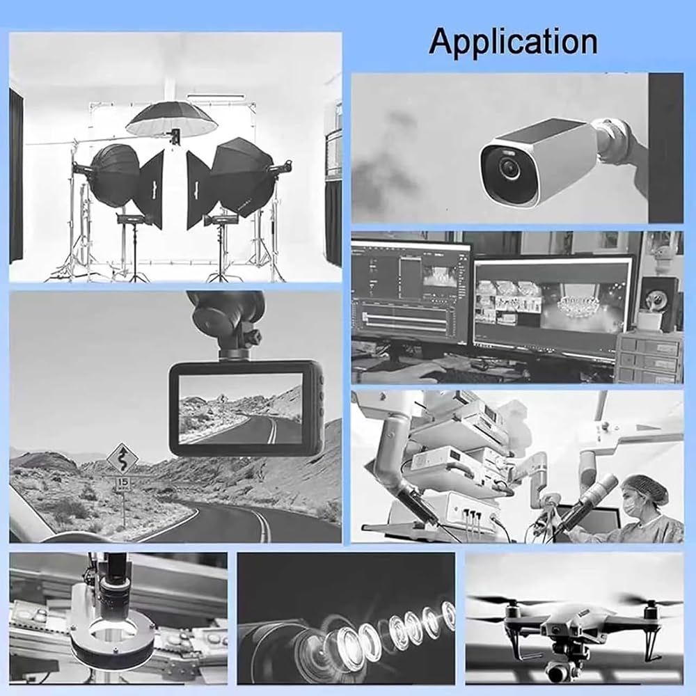
【Multi-scenario optical calibration applications】: Widely applicable for resolution testing, calibration, and quality inspection of various optical devices including cameras, microscopes, and telescopes. Also suitable for comprehensive performance evaluation of image sensors, photographic film, and imaging systems.
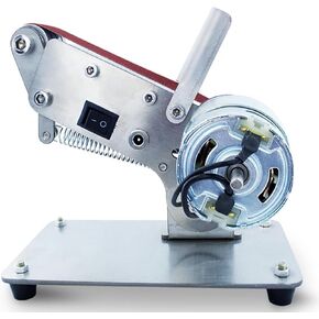 آلة حزام الحزام الصغرى المصغر ، أداة تلميع سطح المكتب الكهربائية مع 7 سرعة قابلة للتعديل ، و 10 أحزمة رمل وتصميم مضاد للانزلاق ومضادة الغبار ، للعمل DIY
SAR 766
آلة حزام الحزام الصغرى المصغر ، أداة تلميع سطح المكتب الكهربائية مع 7 سرعة قابلة للتعديل ، و 10 أحزمة رمل وتصميم مضاد للانزلاق ومضادة الغبار ، للعمل DIY
SAR 766
 آلة إغلاق السيلوفان ، آلة التدفئة اليدوية للسيلوفان ، 7.87 × 7.87 بوصة (200x200mm) جدول تسخين مع شاشة رقمية ، نطاق التحكم في درجة الحرارة 0-400 ℃ ، لتعبئة مستحضرات التجميل
SAR 819
آلة إغلاق السيلوفان ، آلة التدفئة اليدوية للسيلوفان ، 7.87 × 7.87 بوصة (200x200mm) جدول تسخين مع شاشة رقمية ، نطاق التحكم في درجة الحرارة 0-400 ℃ ، لتعبئة مستحضرات التجميل
SAR 819
 مقياس نصف قطر رقمي متعدد الوظائف ، مقياس دائرة نصف قطرها عالية الدقة ، مع 5 فك قياس قابل للتغيير ووظيفة نقل البيانات ، دائرة نصف قطرها (5-700 مم) ، للأجزاء الميكانيكية ، القوالب الخشبية
SAR 1,074
مقياس نصف قطر رقمي متعدد الوظائف ، مقياس دائرة نصف قطرها عالية الدقة ، مع 5 فك قياس قابل للتغيير ووظيفة نقل البيانات ، دائرة نصف قطرها (5-700 مم) ، للأجزاء الميكانيكية ، القوالب الخشبية
SAR 1,074
 مشغل شريط الكاسيت ، كاسيت USB المحمول إلى محول MP3 مع سماعة الرأس ووظيفة التشغيل ، اضغط على زر التشغيل بعد التوقف للتحقق
SAR 527
مشغل شريط الكاسيت ، كاسيت USB المحمول إلى محول MP3 مع سماعة الرأس ووظيفة التشغيل ، اضغط على زر التشغيل بعد التوقف للتحقق
SAR 527

 العربية السعودية