- Shopping, made easy.
- /
- Get the app!
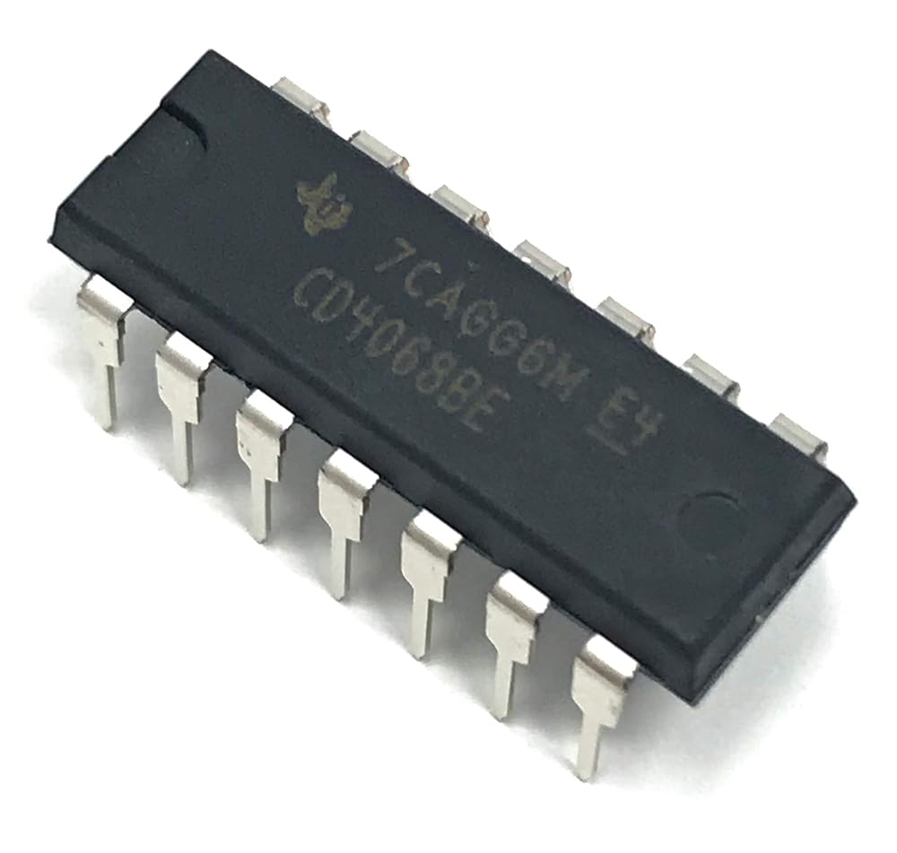
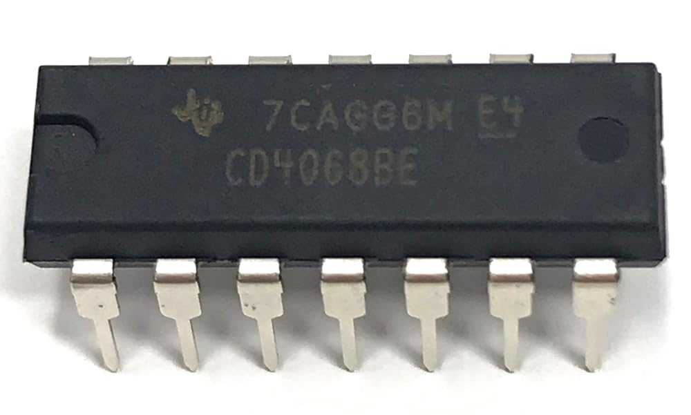
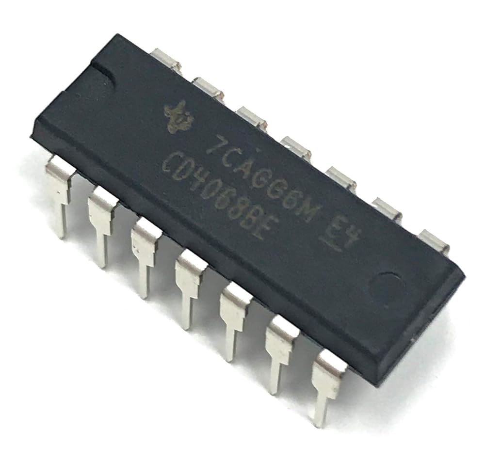
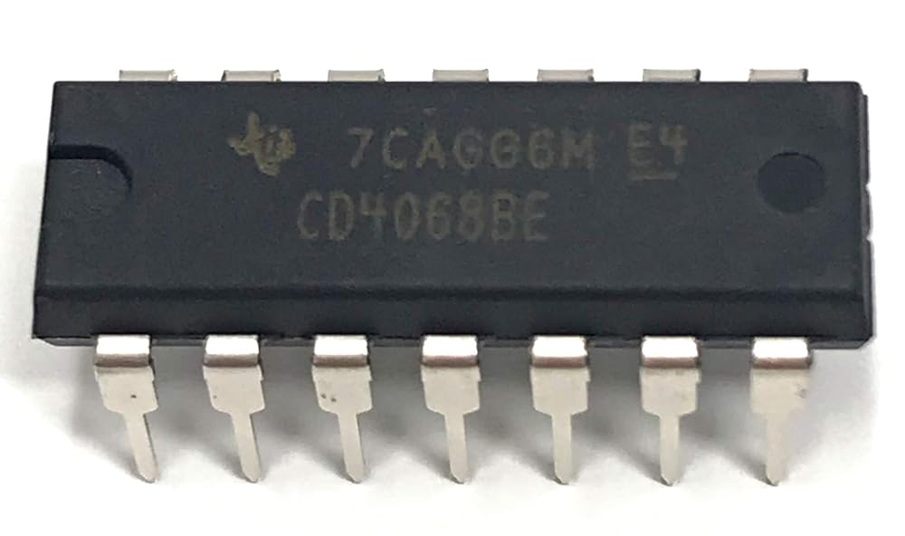
The CD4068B NAND/AND gate provides the system designer with direct implementation of the positive-logic 8-input NAND and AND functions and supplements the existing family of CMOS gates.
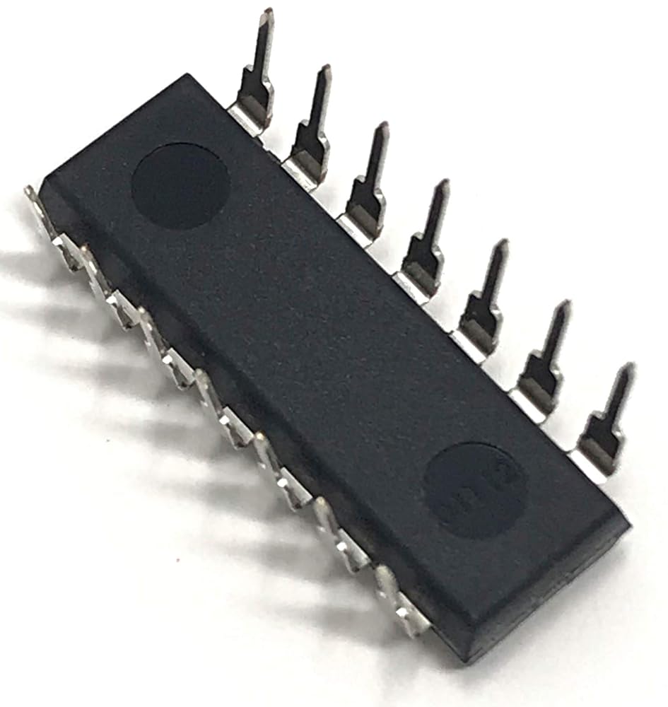
 CD4504BE CD4504B CD4504 CMOS Hex Voltage-Level Shifter for TTL-to-CMOS or CMOS-to-CMOS Operation Breadboard-Friendly IC DIP-16 (Pack of 10)
SAR 79
CD4504BE CD4504B CD4504 CMOS Hex Voltage-Level Shifter for TTL-to-CMOS or CMOS-to-CMOS Operation Breadboard-Friendly IC DIP-16 (Pack of 10)
SAR 79
 LF356N/NOPB LF356N LF356 JFET Input Operational Amplifiers Op Amp Breadboard-Friendly IC DIP-8 (Pack of 5)
SAR 63
LF356N/NOPB LF356N LF356 JFET Input Operational Amplifiers Op Amp Breadboard-Friendly IC DIP-8 (Pack of 5)
SAR 63
 CD4046BE CD4046B CD4046 CMOS Micropower Phase-Locked Loop Breadboard-Friendly IC DIP-16 (Pack of 5)
SAR 65
CD4046BE CD4046B CD4046 CMOS Micropower Phase-Locked Loop Breadboard-Friendly IC DIP-16 (Pack of 5)
SAR 65
 CD4071BE CD4071 CMOS Quad 2-Input OR Gate Breadboard-Friendly (Pack of 20)
SAR 120
CD4071BE CD4071 CMOS Quad 2-Input OR Gate Breadboard-Friendly (Pack of 20)
SAR 120