- Shopping, made easy.
- /
- Get the app!
Product Parameters
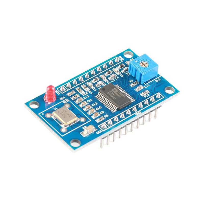
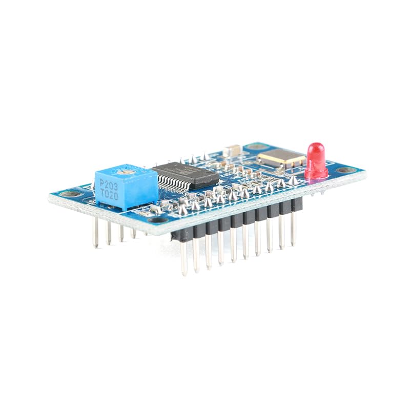
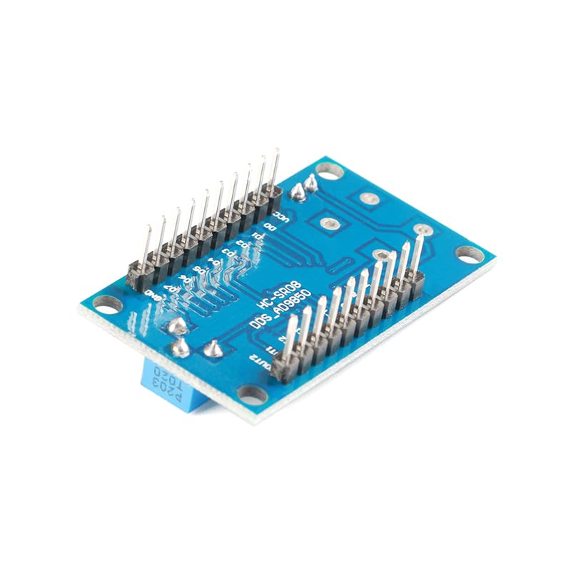
Core Chip: AD9850 DDS Synthesizer
Output Waveforms: 2 sine waves + 2 square waves
Frequency Range:
Sine Wave: 0-40MHz (harmonics increase above 20MHz)
Square Wave: 0-1MHz
Input Voltage: 6V DC (power supply), 3.3V-5V DC (logic control)
Signal Quality: 70MHz low-pass filter for reduced noise
Control Interface: Serial/parallel data input (jumper-selectable)
Dimensions: 45mm × 25mm
Temperature Range: -40°C to 85°C
Key Pin Functions
Power Management:
VCC: 6V DC input (power supply positive)
GND: Power ground
Control Pins:
W_CLK: Serial clock input (rising edge triggers data latch)
FQ_UD: Frequency update (rising edge loads new frequency/phase)
DATA: Serial data input
RESET: Active-high reset (pulse width ≥5 clock cycles)
Signal Output:
IOUT: Sine wave output (current mode, requires 50Ω load)
QOUT: Square wave output (via internal comparator)
Amplitude/Modulation:
DA REF (PIN12): Adjust output amplitude via external resistor
COMP REF: Variable resistor for square wave duty cycle tuning
Common Issues & Solutions
Q1: No output signal detected
Ensure IOUT/QOUTpins are connected to a 50Ω load or buffered amplifier; verify RESETis held low during operation .
Q2: High-frequency sine wave distortion (>20MHz)
Use the 70MHz low-pass filter; reduce output frequency; shorten signal wires and add ground shielding .
Q3: Square wave jitter or instability
Adjust COMP REFvariable resistor for stable duty cycle; check clock stability (≥1% tolerance crystal) .

 10 Sets RT Split Ultrasonic Transceiver Sensor Probe 10 Transmitters + 10 Receivers T+R Ultrasonic Sensor Set 20Pcs Probe Diameter 16mm for Motion Detectionn TCT40-16R/T
SAR 47
10 Sets RT Split Ultrasonic Transceiver Sensor Probe 10 Transmitters + 10 Receivers T+R Ultrasonic Sensor Set 20Pcs Probe Diameter 16mm for Motion Detectionn TCT40-16R/T
SAR 47
 10Pcs IRF520 MOSFET Driver Module MOS Field-Effect Transistor Driver Module Triode for Arduino MCU ARM Raspberry PI
SAR 47
10Pcs IRF520 MOSFET Driver Module MOS Field-Effect Transistor Driver Module Triode for Arduino MCU ARM Raspberry PI
SAR 47
 2pcs CP2102 USB to UART/TTL/RS485/RS232 6-in-1 Serial Module ±0.5% Error -40°C~85°C
SAR 53
2pcs CP2102 USB to UART/TTL/RS485/RS232 6-in-1 Serial Module ±0.5% Error -40°C~85°C
SAR 53
 MusRock MAX9814 Microphone Amplifier Module, 40dB, 50dB, 60dB Selectable Gain, ±0.04% THD, 30nV/√Hz Noise Density, 2.7V–5.5V Power, -40°C to 85°C Operating Range
SAR 42
MusRock MAX9814 Microphone Amplifier Module, 40dB, 50dB, 60dB Selectable Gain, ±0.04% THD, 30nV/√Hz Noise Density, 2.7V–5.5V Power, -40°C to 85°C Operating Range
SAR 42